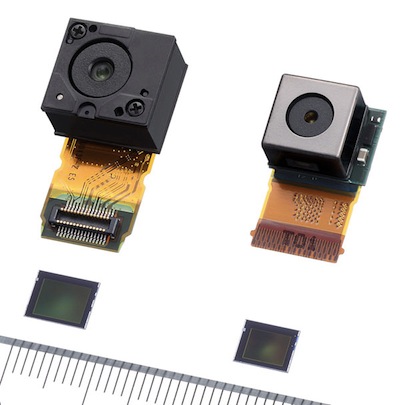
(Above – Exmor sensors for mobile phones)
I’ve been reading some interesting tech documents from Sony related to the image sensor in their latest compacts, the HX5 and TX7.
Since Sony are selling the sensor itself to clients they have a wealth of public domain information on it.
In a nutshell sensitivity and speed are the aims of the Exmor R, which has a back-illuminated structure. Most of the speed increase come from the revised sensor structure allowing column-parallel A/D conversion. Data is therefore output from the sensor quicker due to tiny analogue to digital convertors every line of the sensor.
Back-side illumination improves sensitivity. I believe that noise at the same native ISO is probably similar to normal sensors but the increase in sensitivity improves colour saturation and brightness, probably allowing Sony to have a lower native ISO and a lower boost on the sensor to achieve, say, ISO 1600 equivalent on a CCD sensor. I think this must be the case because the sensitivity claims don’t really stand up when you compare the images from cameras with this sensor to others. They actually look a bit duller than images from the best CCD compacts, like the Canon G10 or Fuji F70EXR.
But the tech is all present and correct. Take it away Sony…
To achieve the resolution of 10.34M effective pixels, the IMX050CQK uses a 1.65 µm unit pixel. When reducing the unit pixel size, light collecting efficiency and increasing the saturation signal level become issues. To resolve these issues, Sony adopted a back-illuminated structure. This structure improves the light collecting efficiency. Sony also optimized the pixel drive to greatly increase the saturation signal. As a result, the IMX050CQK achieves imaging characteristics with a sensitivity of 1262 digits and a saturation signal level of 2721 digits. This corresponds to a sensitivity twice that of current products.
Since the incident light entering current CMOS image sensors passes through gaps in the metal wiring layer, the light is obstructed by that metal wiring layer and cannot be delivered efficiently to the photodiodes. In particular, since light that comes in at an angle is reflected back, problems such as the outer areas of the image being darker or the sensitivity not increasing as the aperture is opened wider occur. Also, when combined with a zoom lens, the sensitivity and color balance of the outer areas of the image may change with the zoom setting.
Sony has now developed a back-illuminated structure that differs from the current pixel structure (the front-illuminated structure) in that the metal wiring layer is placed below the photodetectors. In the back-illuminated structure, light is projected onto the rear surface of the silicon substrate (the back side) and as a result, the amount of light entering each unit pixel is increased since it is not affected by the metal wirings and other circuits. This also allows the change in sensitivity with the angle of incidence to be minimised.
In image sensors, it is easy for electrons that are unrelated to the incident light to be generated from the silicon surface, and even a single electron can become noise of a level that is visible to the naked eye. To avoid this problem, Sony developed a technology that prevents the generation of electrons that occurs at surface defects for this back-illuminated structure in which light is received on the back surface of the wafer.
Furthermore, since light is received on the back surface, it is necessary to transport all the photoelectrons that are generated at the back surface to the circuits on the front surface of the device. Sony also succeeded in developing a unique photodiode with a structure that makes this possible.
Check back soon for my full HD footage from the Sony HX5 equipped with this very same sensor!


